

MODEL 1063 WaferMill™ ion beam delayering solution
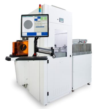
Description
Delayer multiple pre-selected regions on a full wafer from the top down. The fully automated process supports all phases of semiconductor processing for CD-SEM sample preparation.
Key Specifications
- Selected-area milling on full 300 mm wafers
- Top-down delayering
- Expose multiple device layers and structures
- For use in multiple areas of a semiconductor fabrication facility:
– Research and development
– Process control
– Yield enhancement
– Failure analysis
Specification
Application|
Near-line and in-line
Equipment front end module (EFEM)
Manufactured by Brooks Automation; comprises the following:
- 300 mm front-opening unified pod (FOUP) loading station that holds up to 25 wafers
- Four-axis wafer handling robot with a passive end effector
- Pre-aligner that orients the wafer notch based on CD-SEM requirements
- Controller unit
Pre-pump chamber
300 mm VAT valve interface between the EFEM and load lock
UV light
Dual wave-length ultraviolet (UV) light (253.7 nm and 184.9 nm) mounted within the pre-pump chamber
Load lock
A 300 mm VAT valve interface between the pre-pump chamber and the process chamber; wafer presence sensors indicate when a wafer is in the load lock
Vacuum system
Two dedicated turbomolecular pumps; one in pre-pump chamber and one in process chamber
Oil-free diaphragm pump to back turbomolecular pumps
Pressure monitoring with vacuum gauges
Pneumatic supply
Load lock and milling chamber:
- Process gas: Inert gas (argon) with purity of 99.999% (ultra-high
purity); 20 to 30 psi
- Control gas: Dry nitrogen; 60 ±5 psi
- Load lock vent gas: Clean, dry air (CDA); 20 to 30 psi
- Automatic gas control: Three mass flow controllers (one per ion source)
Process chamber
Linear stage moves the wafer in the X and Y direction with 5 µm accuracy
Electrostatic chuck grips the wafer in place to provide a uniform milling plane by eliminating wafer bow
Wafer presence sensors indicate when a wafer is in the process chamber Integrated wafer mapping based on KLARF files
Ion source assembly:
Three ion sources, located 120° apart, at 22.5° from the horizontal plane.
- Variable energy (1.0 to 6.0 keV) operation
- Beam current density: 10 mA/cm2
- Beam size: 2 mm
- Point targeting provides the ability to drive the wafer to any point for processing
Turret/rocking assembly:
- Can be rocked ± 175°
- Angular deviation is ± 5° with a variable step size range of 0.1 to 2°
- Rocking speed is 1 rpm.
Automatic termination
- By timer
- By image processing; milling stops when a specified diameter is reached
User interface
PC-based interface:
- Accessible from EFEM and chamber side
- Used to control the milling process
Operation indicator: Stack light
Optical system
Optical system for beam process monitoring and image acquisition:
- Field of view:
– 15 mm (low magnification)
– 1.4 mm (high magnification)
- Motorized zoom
• Motorized focus
Accesories
Consumables
https://micro-shop.pl/kategoria-produktu/tem/siatki-z-pokryciem-carbon/
For more supplies, please visit our online store Micro-Shop.