

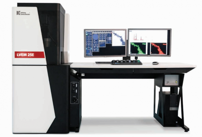
Transmission electron microscope LVEM25E
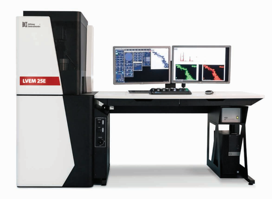
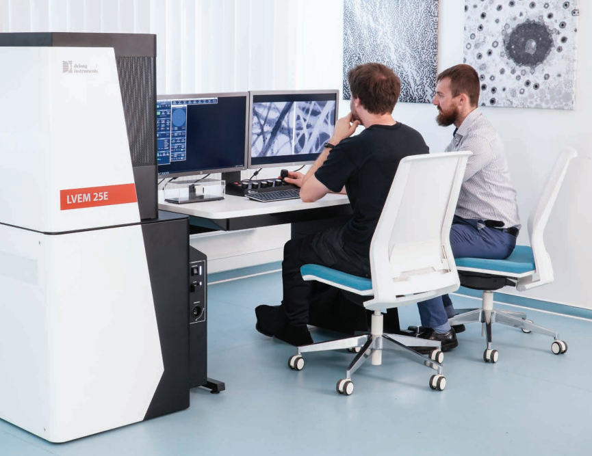
Description
The LVEM25 E microscope is an extended version of the LVEM25 microscope characterized by:
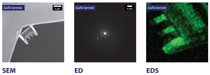
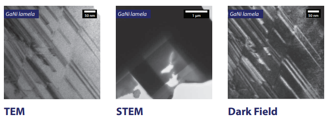
Five imaging modes in one instrument
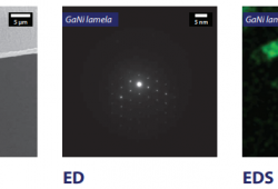
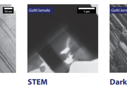
- Equipped with TEM, STEM, SEM, EDS and ED modes V Easily switch between imaging modes via intuitive software
- Bright and dark field measurements in both TEM and STEM modes
- SEM mode (BSE) for surface measurements V Energy Dispersive Spectroscopy (EDS) for elemental analysis
- Electron Diffraction (ED) for understanding crystal structure
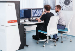
Fully integrated and portable design
- Extremely compact, space-saving and portable design
- Single-plug installation in nearly any laboratory environment
- No special facility requirements (no cooling, power or anti-vibration isolation needed)
High contrast and resolution for standard samples
- Unmatched contrast of biologic and light material samples
- Meaningful results with reduced staining
- Image resolution as good as 1.0 nm
- Designed for conventionally prepared samples
Super-fast sample exchange
Specification
OPERATION
- Electron gun Schottky: field emission gun
- Specimen size Standard Ø 3.05 mm TEM grids
- Objective lens Magnetostatic
- Projective lens Electrostatic
- Specimen movement x, y: ± 1 mm z: ± 0.5 mm
- Tilt holder ± 6°
IMAGING MODES
TEM
- Nominal accelerating voltage 25 kV
- Resolution 1.0 nm
- Total magnification* 3,400 – 1,300,000×
- Magnification in Low mag regime* 1,500×
- Field of view 100 – 0.25 μm
- Field of view in Low mag regime 225 μm
TEM IMAGE CAPTURE
- Camera sCMOS
- Sensor size 2,048 × 2,048 pixels
- Digitalization 16-bits
ELECTRON DIFFRACTION
- Probe size 500 – 8,000 nm
- Camera length (binning 2×2) 2,000 – 5,000 pixels
- Camera constant (binning 2×2) 17 – 40 nm pixels
STEM
- STEM 10 or STEM 15
Nominal accelerating voltage: 10 kV or 15 kV - Resolution: 1.0 nm or 1.3 nm
Maximum magnification: 940,000× or 750,000× Maximum field of view: 105 μm or 80 μm
SEM (BSE DETECTOR)
SEM 10 or SEM 15
- Nominal accelerating voltage: 10 kV or 15 kV
- Resolution: 10 nm
- Maximum magnification 940,000× or 750,000× Maximum field of view: 105 μm or 80 μm
EDS
- Detector type: Silicon Drift Detector (SDD)
- Detector active area: 30 mm2
- X-Ray Window Windowless
- Energy Resolution: Mn Kα ≤ 129 eV
- Maximum throughput: 130 000 cps
- Hardware integration: Fully embedded
- Software: Esprit 2.3
Consumables
https://micro-shop.pl/page/6/?s=siatki+TEM&post_type=product