

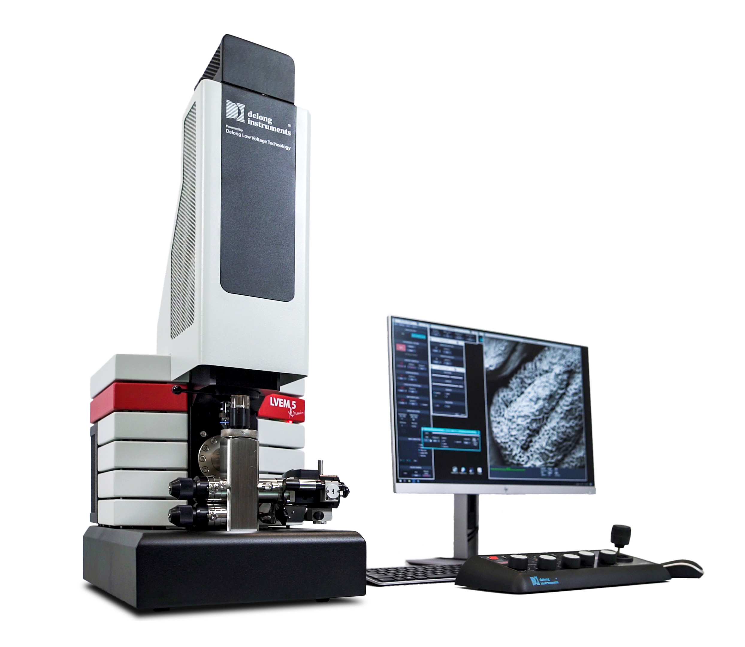
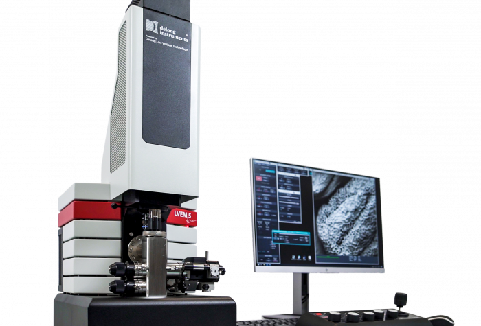
Transmission electron microscope LVEM5

Description
The LVEM5 is designed to excel across a broad range of applications in material sciences, such as nanomaterials, polymers and biomaterials, and in life sciences, such as drug discovery and delivery, pathology and virology. The LVEM5 offers a high throughput benchtop solution with nanometer resolutions.
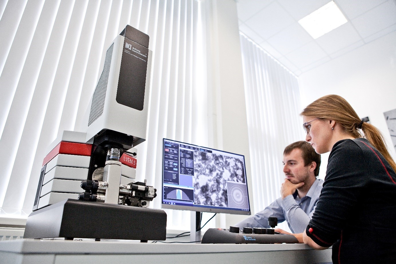
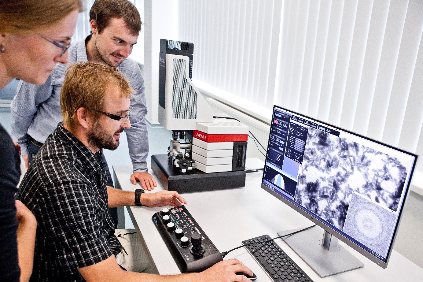
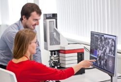
The LVEM5 has an architecture that departs from traditional models. The benchtop design alone is a significant architecture and footprint departure from classical TEM design. The LVEM5 is approximately 90 % smaller than classical electron microscopes. This means that the LVEM5 can be installed in a lab, on a desktop or benchtop; almost anywhere electron imaging is needed. It features a small footprint and is easy to service. There is no need for a dark room or cooling water.
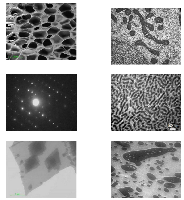
The LVEM5 is a unique investigative tool which combines transmission (TEM, STEM) and surface scanning (SEM) observation modes. High contrast on light elements comes from the 5 kV accelerating voltage, which is substantially lower than in conventional TEM (typically 80–200 kV). This results in increased electron scattering and enhanced contrast on biological, organic and light materials
- unique concept of S / TEM bench microscope with compact dimensions
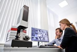
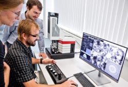
- extremely easy to use – ideally suited for research and teaching purposes;
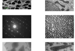
- enables high performance imaging in TEM, STEM, ED, SEM modes;
- ensures high contrast of obtained sample images – without the need to stain biological samples;
- microscope inexpensive to operate – due to advanced vacuum system and S-FEG emitter with a long service life, service operations on the device are limited to a minimum
an excellent solution for imaging nanoparticles, stained and unstained biological and polymer samples, powders, fibers or nanotubes;
Specification
- electrons source with Schottky cathode (S-FEG) with a lifetime of> 2,000 hours;
- accelerating voltage 5kV;
- time from sample insertion until the first photo is obtained ≤ 3 minutes;
- in the TEM imaging mode:
- resolving power ≤ 1.2 nm;
- maximum magnification ≥ 700,000x;
- saved images with a resolution of up to 2,048 x 2,048 pixels;
- in the STEM imaging mode:
- resolving power ≤ 2.5 nm;
- maximum magnification ≥ 250,000x;
- saved images with a resolution of up to 2,048 x 2,048 pixels;
- in ED diffraction mode:
- minimum beam diameter ≤100nm
- camera length 2100pix
- in SEM imaging mode:
- resolving power – 3 nm;
- maximum magnification ≥ x 100,000;
- saved images with a resolution of up to 2,048 x 2,048 pixels