

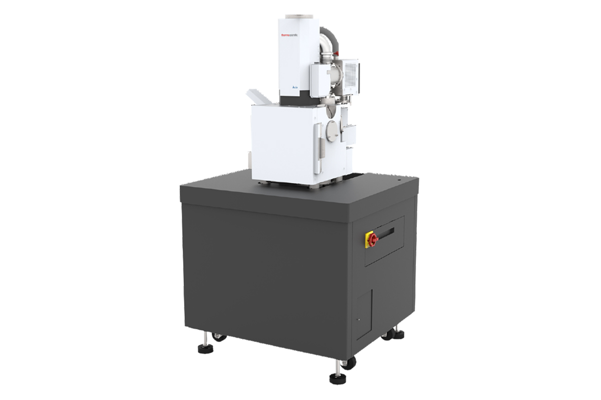
Axia ChemiSEM
Description
Even though scanning electron microscopy (SEM) has made tremendous advances, it can be considered by new users to be a complicated technique. Sample preparation, alignments, cost of ownership, and difficulties with analytical techniques prevent widespread adoption. We set out to resolve these challenges in order to make a truly accessible SEM without compromising on flexibility. Our goal was to make microscopy an easy and enjoyable experience in which you should not have to fight the microscope to obtain quality data. The result is the Thermo Scientific Axia ChemiSEM™ Scanning Electron Microscope, a system in which obtaining SEM-EDS data is no longer a chore. EDS is no longer just an afterthought—chemical data and imaging have now become one.
The Axia ChemiSEM is unlike traditional SEMs in that it always collects EDS data in the background. It uses unique algorithms to process the SEM and EDS signals simultaneously, allowing it to display the morphology and quantitative elemental make up of a sample together, in real time. It constantly processes EDS data in the background, giving you live updates on elemental data, as it is acquired. Elements found in your sample can be toggled on and off, allowing you to isolate areas of interest.
The Axia ChemiSEM features a superior user experience enhanced by automation, such as SmartAlign technology for alignment-free operation, newly developed automatic functions, and live quantitative EDS mapping. This always-on processing make analysis twice as fast, compared to traditional methods. The Axia ChemiSEM Scanning Electron Microscope puts SEM/EDS analysis within reach of a wider scientific audience, speeds up your workflow, and saves time on training.
Specification
| Standard |
|
| Electron beam resolution |
|
| Chamber |
|
| Stage |
|
| Common options |
|