

TEM nanoscale strain mapping autostrain
Description
Novel Automated Strain Mapping Solution for TEM/STEM (Patent pending) based on nanobeam precession diffraction patterrns in combination with DigiSTAR. Precision up to 0.02% (200kV FEG) with spatial resolution up to 2nm attainable (FEG-TEM).
In combination with TOPSPIN simultaneous orientation/ phase/strain/STEM maps are possible

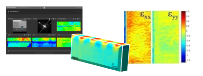
Strain maps from the Si regions of a pMOS device
- x and y-directions aligned with [220] and [002] directions in Si.
- Localized biaxial tensile strain close to contact edges.
Strain profile of an Si/SiGe layer
- Strain in x-direction is near zero, indicating a coherent interface
Specification
Features:
• High spatial resolution, high precision strain mapping in modern semiconductor devices
• Acquisition of STEM reference image
• Ultra-fast nanobeam precession electron diffraction scanned acquisition
• Typical acquisition time: 5-10 min (150×150)
• Time per pixel: 10-40 ms Analysis time 5-10 min
• Automated local strain analysis via AppFive proprietary algorithm
• Acquisition from individual positions, line profiles, areas
• Spatial resolution < 2 nm attainable (FEG TEM)
• Monitor engineered strain distributions in modern semiconductor devices
• Expected sensitivity : < 2 x 10⁻⁴
• Intuitive workflow
Consumables
https://micro-shop.pl/kategoria-produktu/tem/siatki-z-pokryciem-carbon/
For more supplies, please visit our online store Micro-Shop.