

NANO – Robotics Solutions for Electron Microscopes
Description
Integrated nanoprobing solutions for SEM and FIB. Bring probe tips in contact with semiconductor chips, measure the electrical characteristics of integrated components, localize defects and isolate structures.
Imina Technologies’ NANO solutions are turnkey for electrical characterization of microelectronic devices, in situ semiconductor failure analysis and manipulation of single structures in SEM and FIB chambers. Fully controlled from Precisio™ software suite, comprehensive workflows provide operator assistance from setting up the system, to landing probe tips on the device under test, acquiring and processing measurements and reporting.
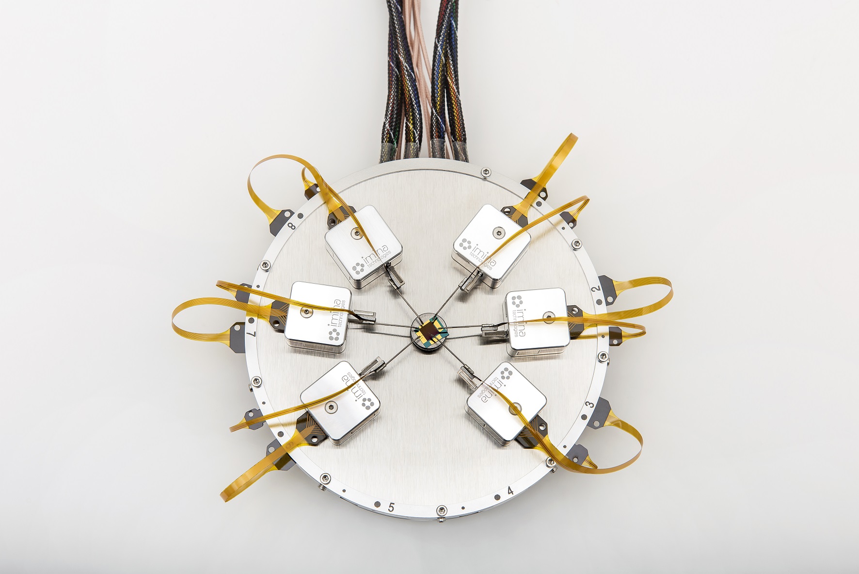
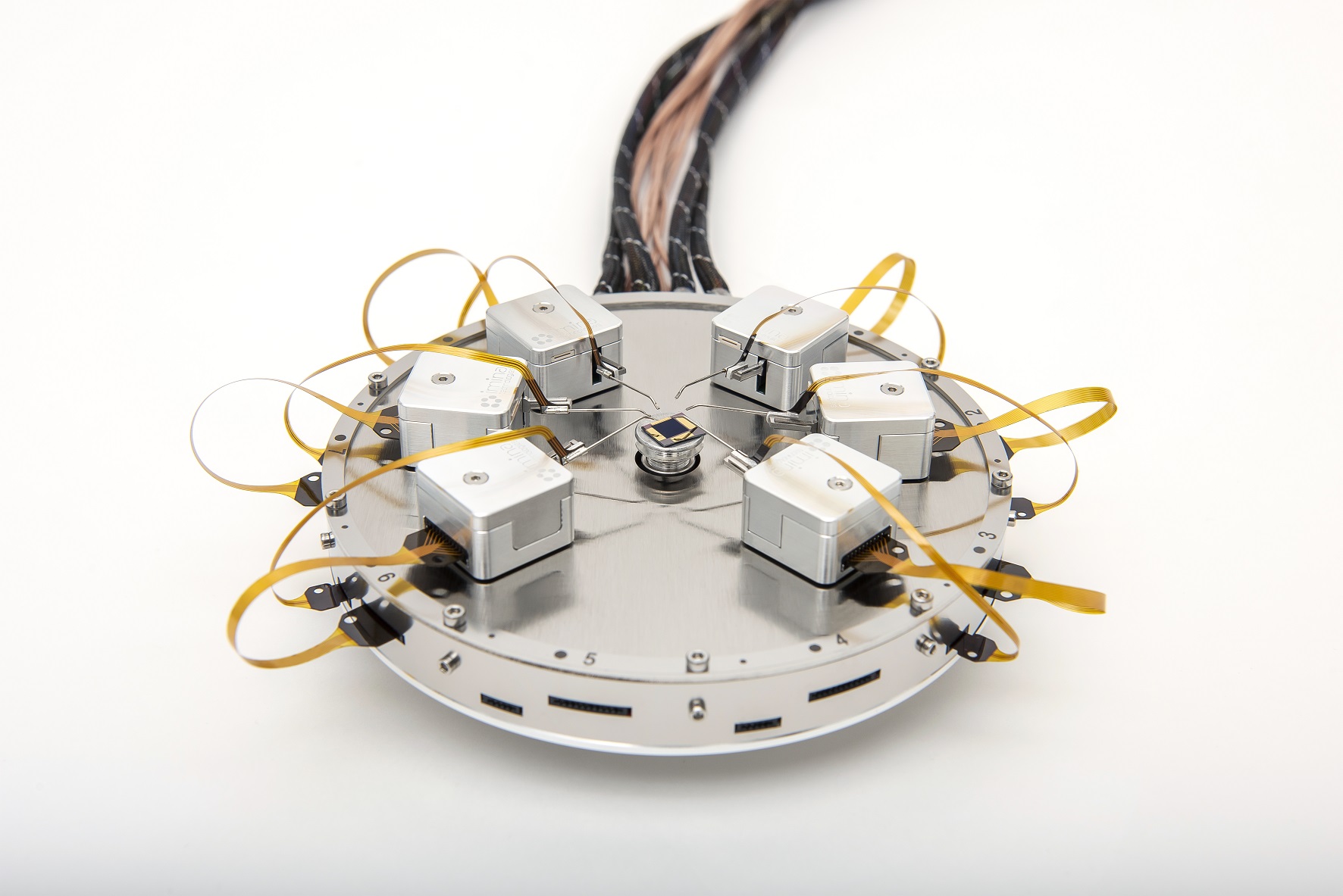
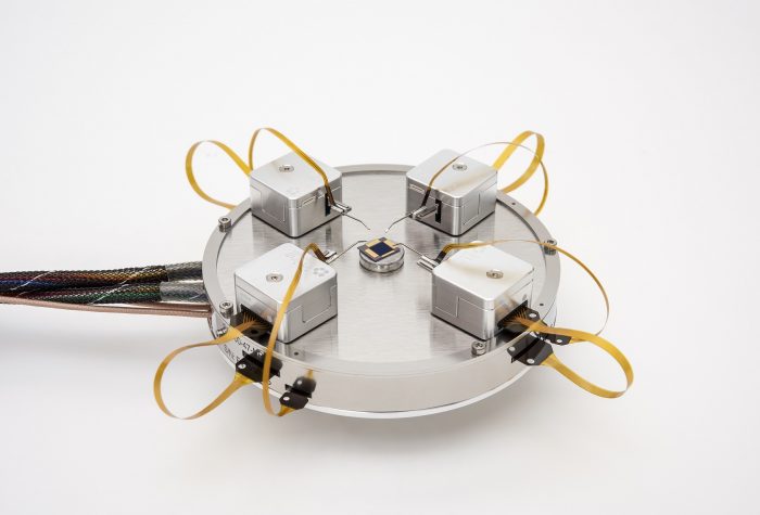
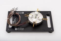
Up to 8 miBot™ nanoprobers can be delivered with various configurations and options to adapt to application specific requirements and equipment setups.
The compact and light platforms for the robots are compatible with any electron microscope and can either be mounted on the SEM sample positioning stage, or be loaded via the SEM load-lock.
The compatibility with high resolution imaging using magnetic lenses enables the operator to perform nanoprobing experiments with the most advanced scanning electron microscopes on the market and take advantage of the highest resolution imaging capabilities, even at accelerating voltages below 0.5 kV.
As the whole platform and robots can be tilted, in situ FIB circuit editing and nanoprobing can be performed simultaneously providing faster and more accurate failure analysis results.
No permanent modification of the chamber is required and the installation and removal of the system only takes a few minutes. This avoids to dedicate an SEM for nanoprobing. Also, various extra accessories exist to easily operate the main components of a NANO solution under optical microscopes such as probe stations and inspection tools, increasing the value of your investment.
Applications:
Semiconductor characterization
─ I/V curves of single transistors
─ Bit cell memories characterization
─ IC attacks for cybersecurity, reverse engineering
Failure Analysis (FA)
─ EBIC: Electron Beam Induced Current
Defects localization at p/n junction
─ EBAC/RCI: Electron Beam Absorbed Current
Shorts/Opens detection at metal lines
Materials characterization and nano-manipulation
─ 4-point probing on single structures
─ Thin-film characterization
─ Single structure isolation (nanowires, particles, etc), TEM sample preparation
Specification
Degrees of freedom
4 independently driven (X,Y,R,Z) per probe
Dimensions & weight
Body: 20.5 x 20.5 x 13.6 mm3
Arm: 8.3 mm (without tool)
Weight: 12 g (without tool)
Max. positioning resolution:
Motion modes: coarse (stepping) and fine (scanning)
Stepping: 50 nm (X, Y), 120 nm (Z)
Scanning: 1.5 nm (X, Y), 3.5 nm (Z)
Motion range
Stepping (XY,R,Z): 20 x 20 mm2 , ± 180°, 42°
Scanning (X Y Z): 440 x 250 x 780 nm3
Note: in stepping, actual X, Y, R range are limited by the size and shape of the stage where the miBot moves, and the length of the driving cable.
Speed
X and Y: up to 2.5 mm.s-1 Z: up to 150 mrad.s-1
Forces & torques
X and Y: push: 0.3 N Z: lift: 0.7 mNm (5 g)
hold: 0.2 N hold: 0.9 mNm (6 g)
Tilt angle Holding position up to 55°
Tool holders
Range of holders for probes and optical fibers
Accesories
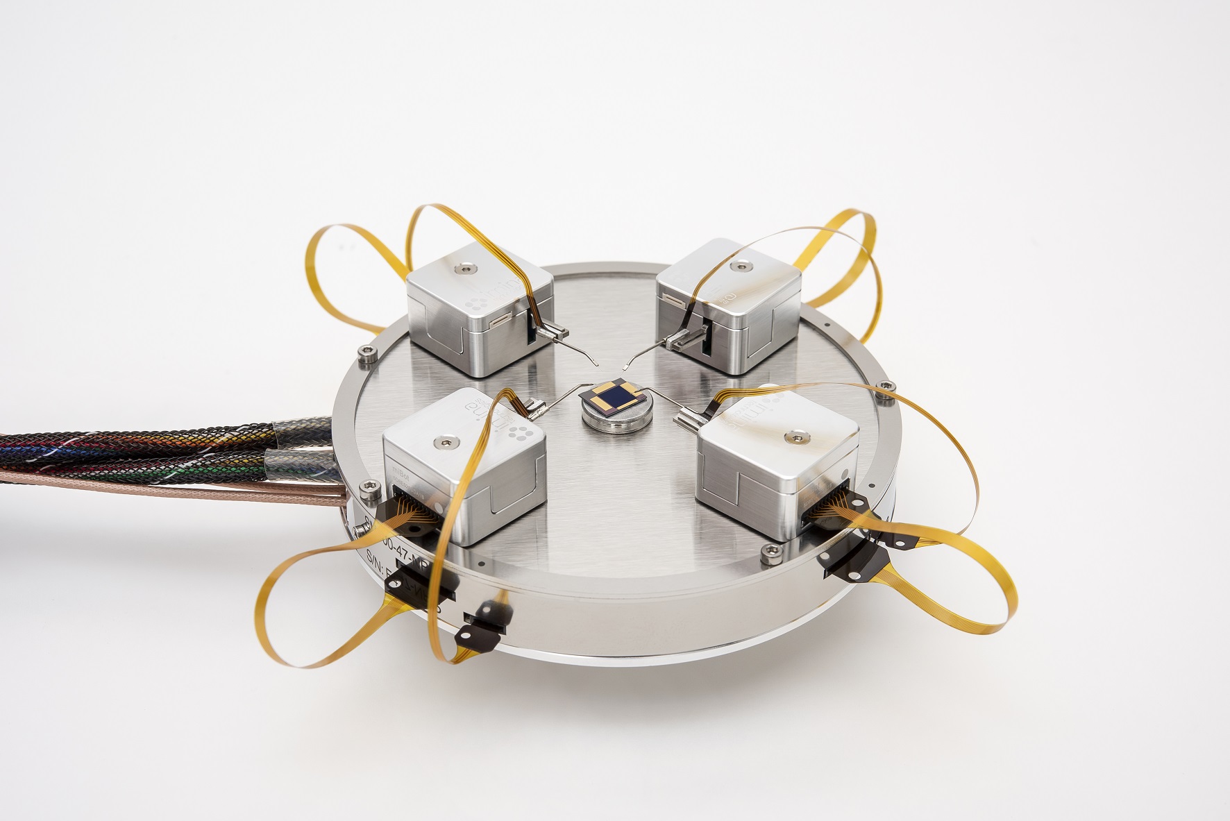
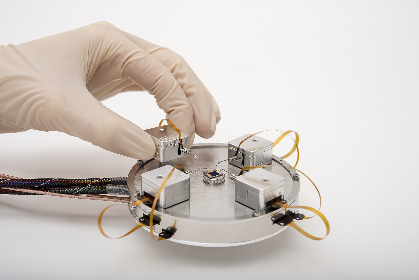
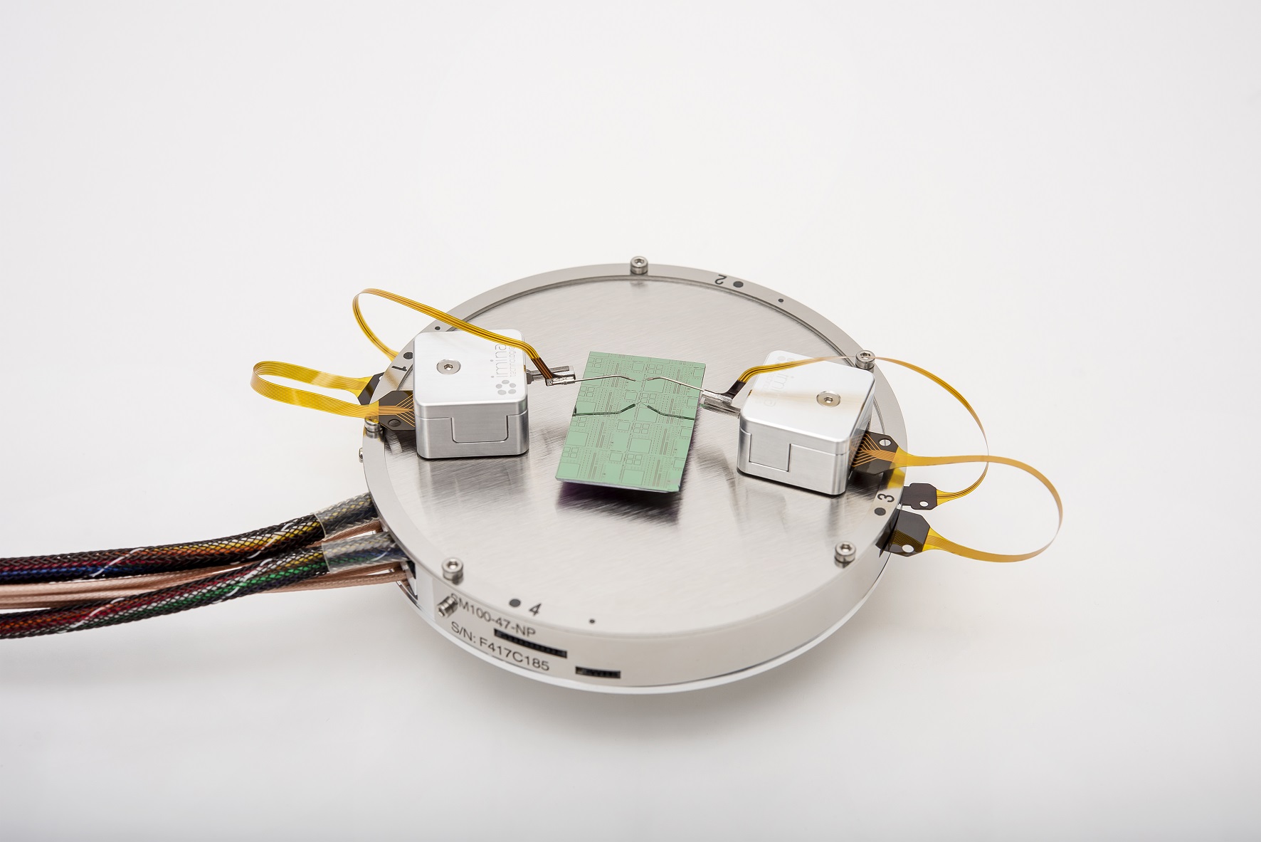
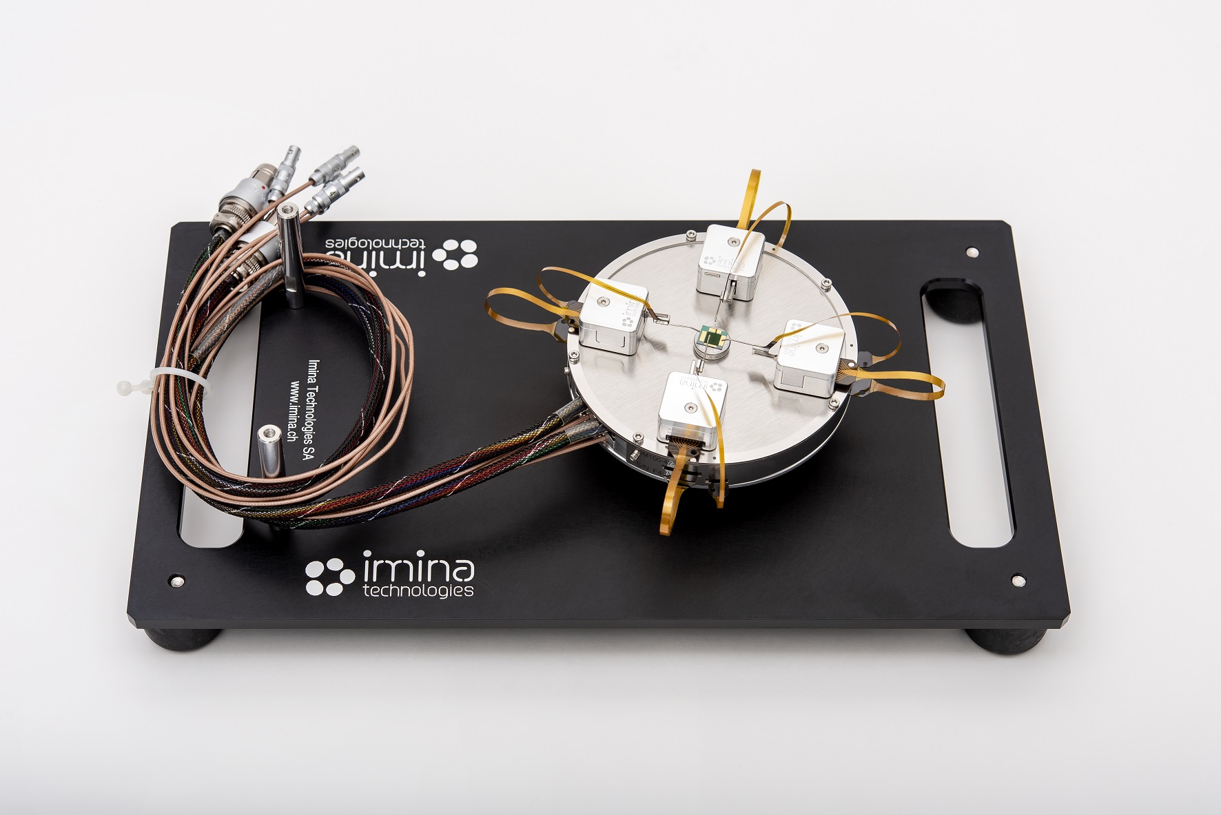
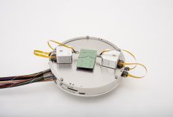
Stage mounted platform 4-Bot
•Compact design (diameter: 100 mm)
• Up to 4 independently driven miBot™ nanoprobers
•Sample size up to approx. 1”
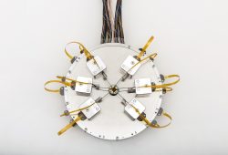
Stage mounted platform 8-Bot
•Wide design (diameter: 125 mm)
•Up to 8 independently driven miBot™ nanoprobers
•Sample size up to approx. 2”
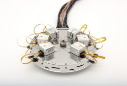
Load-lock platform 8-Bot
•Wide design (diameter: 110 mm)
•Up to 8 independently driven miBot™ nanoprobers
•Sample size up to approx. 1.5”
• Typical airlock door inner dimensions:
150 (w) x 45 (h) mm
Special platform integrations
•For large/thick samples (e.g. packaged chips)
• With heating/cooling sample stages
•Custom chamber set-ups (e.g port-mounted)
Active sample holder:
•Manual sample height adjustment (8 mm range)
•User defin ed specimen biasing
Sample positioning XYZ sub-stage
• Move the sample independently from the probes
in X, Y, Z directions (travel range: 5 mm (X, Y),
330 um (Z); max. resolution: 2 nm (X, Y), 7 nm (Z))
• Reduce probes landing time and accelerate multiple
device characterization
•User defined specimen biasing
Additional SEM integration kits
Install your nanoprobing system in minutes and
operate in any of your microscopes by preinstalling
the interface parts on the different chambers.
EBIC acquisition system
High performance external current amplifier and
SEM image acquisition system for quantitative
EBIC capabilities
EBIC & EBAC/RCI acquisition system
Best in class in situ and ex situ preamplifiers
combined with integrated scan generator and
SEM image acquisition system for quantitative
EBIC and low noise EBAC/RCI analyses